Wafers of sand
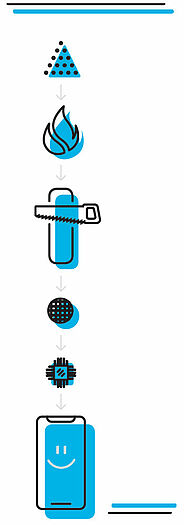
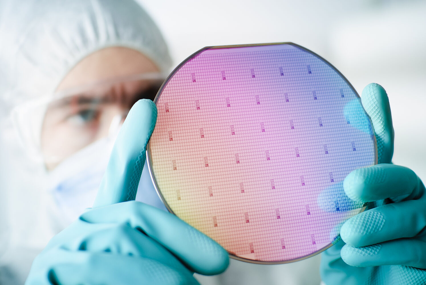
The raw material for chip manufacture could hardly be simpler: sand, quartz sand to be precise. The sand is first melted, and other constituent parts are separated from the main component, silicon. A so-called seed crystal from the same material initiates crystal growth in the liquid mass. Cylindrical rods with homogeneous structure are created. Discs about two millimetres thick are cut off from these: the raw wafers. After some smoothing and polishing, the blanks are coated with a photosensitive lacquer. The conductor paths, the thickness of which in modern chips is in the nanometre range, are created with a photolithographic process and subsequent etching of the material.
The complex structures, which connect millions of transistors on a chip to form an integrated circuit, are thereby created. Each unit is exposed up to thirty times with different photomasks. The many dozens of units on the wafer must be exactly aligned with those from the previously performed exposure. In this multi-stage process, the chip structures then appear on the round disc, which is similar in appearance to a wafer and the source of its name.
Robots move the wafers during all steps and guide them to the various process steps. The blanks are highly sensitive and must not bump into anything anywhere in spite of what are usually constrained spaces in the systems. In order for error-free structures to be created, their alignment must be extremely precise. The same holds for the optical components of the lasers in the photolithographic systems. Ensuring the precise movement of the components with reliable reproducibility in the robots and in the lasers are drives from FAULHABER, such as DC, stepper or piezo motors.
Wire and synthetic resin
After the structures in the crystalline silicon have reached their final form, the individual chip blanks are cut from the wafers. These now receive their electrical connections (pins) in the form of fine wires made of aluminium or gold. They are unwound from rolls, a process that is, of course, also fully automatic. A special machine is responsible for this production step, the so-called wire bonding. It guides the wire end to the desired location, unwinds and cuts the required quantity and performs the soldering.
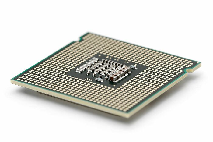
The chips are then enclosed by a protective shell, usually made from black synthetic resin. The process is similar to plastic injection moulding only that here very high precision is again required. The quantity of synthetic resin must be precisely dosed in order to effectively protect the circuit yet also ensure that nothing protrudes that could inhibit installation or function. Dosing is therefore performed by a motorised unit: the usually black synthetic resin passes through a spindle, the forward motion of which transports it toward the injection mould. After travelling an exactly measured path – in the millimetre range – the motor switches to reverse so that a precisely defined quantity of resin can be released and enter the mould. Once this process has been completed, the circuits have their characteristic appearance: the chip is now finished and is tested in the so-called test handler.
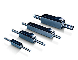
In this machine, a pick-and-place robot is responsible for transporting and placing the chips in the testing devices. Since parts are processed here that are no more than a few square centimetres in size, the dimensions of the system parts are also correspondingly delicate. The motors for their movement must be extremely compact but also be able to deliver very high acceleration values. The same applies for the wire bonding mentioned above. In both cases, the motors must perform their work with the utmost precision. Because the requirements are so high, motors from FAULHABER, such as the BX4 series with integrated Motion Controller or the portfolio of linear DC-servomotors, are used in many machines in this process area.
Rapid assembly and needle test
The tested chips are usually packed in plastic belts and are then transported to the next stage in microelectronic manufacturing: to the assembly of the PCBs. You are no doubt familiar with these usually green plastic boards with chips, various other electronic components, copper conductive pathways and shiny, silver-coloured solder points – after all, we encounter them literally everywhere. Together with the components that hold and connect them, they form the small or large computer units that are responsible for flawless function not only in computers and smartphones but also in every car, in every household appliance, in every machine and in countless other products. Mass production prevails here as well: countless components are mounted on PCBs every day.
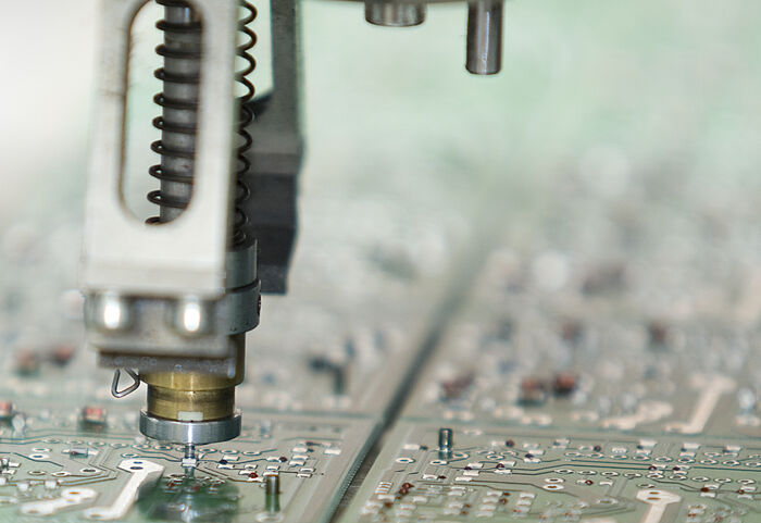
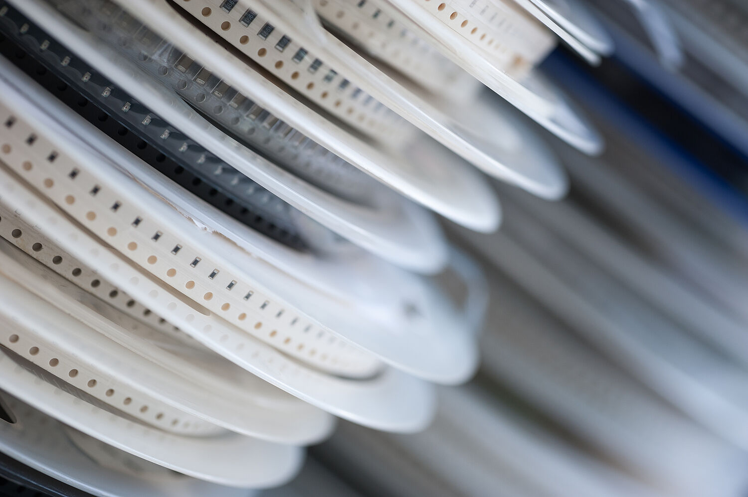
This work is performed by automatic placement machines. The belts with the components are fed to the mounting stations on rollers. Small pockets in the belt hold the components, a perforation at the edge of the belt enables precise transport. The belt is unrolled so that the placement head can always pick up one component. This last step is generally performed under negative pressure: the component is drawn in and held in the same manner. The head then moves to the location on the PCB at which the appropriate openings for the connections of the chip or other component are located. It places the chips on the openings; later they are soldered to the board.
It is easy to imagine how sensitive the hair-thin connections are. Any misplacement, even a faction of a millimetre, would bend and, thus, destroy them. Here, too: precision has top priority. At the same time, a large throughput is required for the massive quantities. Some machines manage over 100,000 components per hour. The bare eye sees only the shadow of the tremendously rapid movement here. The demands on the motors that move the conveyor units and the mounting heads are similar to those in the other areas of microelectronic production.
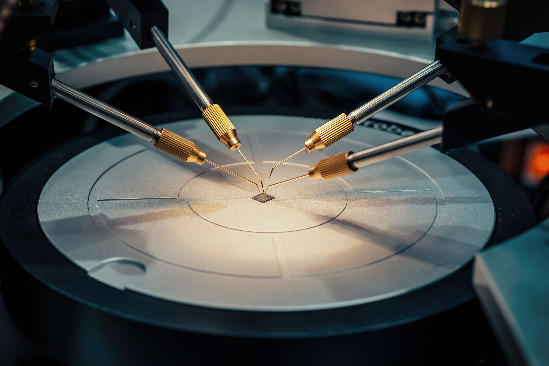
The subsequent quality inspection must also be extremely fast, as each individual PCB is thoroughly tested. The electrical conductivity of the connections provides information about the proper function of the circuits. To measure it, extremely small needles are guided to individual – two or more at a time – connections and placed under voltage. This is repeated for each part until all conductive pathways have been checked over. This process cannot be envisioned as a leisurely testing operation, however: the boards are often produced by the million. The fully automatic testing machines must therefore be able to handle a large throughput. The movement of the needles, for example, is so fast that it can only be followed in super slow motion.
Products
